CS31 Lab 3: Circuits
Part 2: Due before midnight Tuesday, Feb. 20
Lab 3 Goals:
- To build and test digital circuits.
- To understand how machine code instructions are executed by digital circuits.
- To apply incremental implementation and testing to circuit design.
Contents:
You will have the same partner for both parts of this lab.
The course webpage has a section on expectations for working with partners.
Both you and your partner should:
- On the CS system, cd into your cs31/labs subdirectory
cd ~/cs31/labs
- Get your Lab03 ssh-URL from the GitHub server for our class: CS31-s18
- Clone a local copy of your shared repo in your private
cs31/labs subdirectory:
git clone [your_Lab03_URL]
README.md QUESTIONNAIRE alu.circ part1.circFor more detailed instructions see the the Using git guide.
As you and your partner work on your joint solution, you will want to push and pull changes from the master into your local repos frequently.
Merge conflicts in logisim .circ files will be difficult to resolve by hand, so it is extra important this week that you and your partner take turns editing.
In this lab we will use Logisim to design and simulate circuits. See the Beginner's Guide and Library Documentation of the Logisim web page (version 2.7.x) for more help.
All the circuits for this part should be in a single file named part1.circ. There are logisim circuits that do sign-extension and addition. You should not use these for part 1. Instead, build the part 1 circuits using only AND gates, OR gates, NOT gates, input pins, output pins, and splitters. It's okay to use AND and OR gates with more than two inputs.
Run the following command to open the part1.circ starter file in Logisim:
$ logisim part1.circ
Edit the text at the top of this file to list your name and your partner's name.
Sign Extension
Sign extension is an common operation performed inside a CPU. It is used when a value stored in a register uses fewer bits than the register's capacity. Create a circuit (Project→Add Circuit) that takes a 2-bit 2's complement number and performs sign extension so that the output is an equivalent 4-bit 2's complement number. Name this circuit signext2to4. Be sure to label each of your input and output pins. Your input should be labeled so that the least significant input bit is a0 and the most significant input bit is a1. Following the same pattern, label your output bits b0 through b3.
1-bit Full Adder
Create a 1-bit full adder as a new circuit (Project→Add Circuit). Name this circuit fulladder. Your full adder should take 3 inputs (x, y, carry-in) and yield two outputs (sum, carry-out).
Start with the truth table for x + y + carry-in = sum, carry-out and then translate this into a circuit.
Test your circuit for all possible inputs.
4-bit Full Adder
Add a new circuit, fulladder4, that takes two 4-bit input values, x and y, and one 1-bit input value, carry-in, and produces a 4-bit sum output value and a 1-bit carry-out value. To build this circuit you should use four copies of your 1-bit adder. x and y should each be represented with an input pin with the "Data Bits" option set to 4. You can then use a splitter to get the value of each bit. You can also use a splitter facing in the opposite direction to collect the four 1-bit output wires into the 4-bit output value, sum.
Test out your 4-bit adder for different input values.
NOTE: The 4-bit adder you are building adds two 4-bit numbers, whether they are unsigned or 2's complement. The only difference has to do with overflow, which you aren't dealing with in this question. The addition is the same either way.
Putting it all together
Finally, add a circuit named tester. Add copies of your 4-bit adder and your sign extender into this circuit. You are going to build a test circuit with 3 input values:- One 4-bit value: x
- One 2-bit value: y
- One 1-bit value: carry-in
- One 4-bit value: sum, the result of x + y
- One 1-bit value: carry-out
Test out your resulting circuit for different input values. The three inputs and two outputs should all be represented as pins in the circuit design you submit. You can figure out whether one of your components is a pin by selecting it and looking at the attribute table that appears in the lower-left portion of the logisim window.
When you're working with 1-bit wires, logisim uses color to indicate whether current is flowing through the wire or not. Your tester circuit will have wires carrying more than a single bit. To examine the value flowing through a multi-bit wire you can attach a "Probe" to it. This will be a useful debugging aid here and especially in part 2.
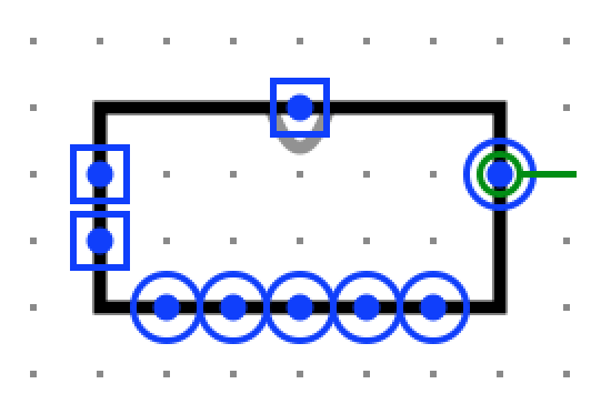
One last thing before you submit: We will be able to grade your assignments much more efficiently if everyone submits a circuit that appears the same when used as a subcircuit in a larger circuit. Right-click on the name of your tester circuit where it appears in logisim's explorer pane. From here you can alternate between editing the circuit's appearance and editing its layout. Edit your circuit's appearance so that it is identical to ours:
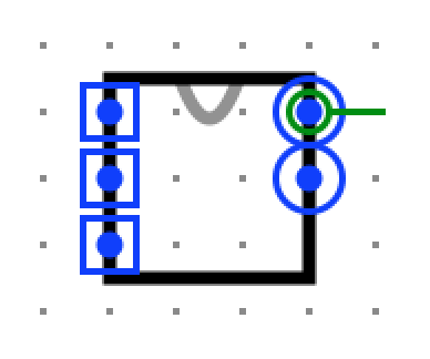
Now make sure that your inputs and outputs appear in the following order: going down the left side of the circuit, x, y, and carry-in; going down the right side, sum and carry-out. You can verify this by using your tester circuit as a subcircuit in the main circuit and hovering over the connection points until the corresponding labels appear.
In this part of the lab, you will implement an arithmetic logic unit. Your answer will be stored in alu.circ in the circuit labeled main. The ALU is the part of the processor that performs mathematical and logical operations. Unlike in part 1, now you can and should use whatever components from Logisim you want. For example, do not build a 8-bit adder--instead use the 8-bit adder that is already part of Logisim.
To use an 8-bit adder, open the "Arithmetic" folder and select "Adder". The default Adder has "Data Bits" set to 8. The inputs to an 8-bit adder should also be 8 bits wide, so you need to hook up an 8-bit input pin. The output is 8-bits, so you need to hook up an 8-bit output pin. The carry-in and carry-out bits are 1-bit each.
Requirements
Your ALU should perform 8 arithmetic functions on two 8-bit inputs, producing one 8-bit output, and five 1-bit outputs (condition code flags). In addition it will have one 3-bit input, the opcode, which selects from the 8 arithmetic functions. Implement this in your circuit using a multiplexor with 3 "Select Bits" and 8 "Data Bits". The correspondence between opcodes and functions is as follows:
- 000: x or y
- 001: x and y
- 010: x + y
- 011: x - y. Logisim contains a Subtractor circuit, but you should not use it. Instead use another Adder circuit to perform subtraction: instead of x - y do x + ~y + 1. Under "Wiring", there is a "Constant" component that you can use for the c_in input to the Adder circuit.
- 100: x <<y. Shift x to the left y times. e.g. 10111000 << 00000001 is
01110000. Logisim has a "Shifter" gate that can be
customized to perform this and the next two
operations. The second input to the Shifter can only
be 3 bits. Use a Splitter to extract the last three bits of
y. You can adjust the Splitter's attributes so that it selects exactly these 3
least significant digits. The
"Fan Out" attribute determines how many outputs there are from the
splitter and the "Bit #" attributes specify to which
output each of the input bits go. Note that "None" is an option here.
- 101: x >>y (Shift right) without sign extension (also known as logical shift), e.g. 10111001 shifted right by 1 is 01011100, not 11011100. Use the last three bits of y.
- 110: x >>y (Shift right) with sign extension (also known as arithmetic shift), e.g. 10111001 shifted right by 1 is 11011100 and 01000001 shifted by 1 is 00100000. Use the last three bits of y.
- 111: x < y? The output should be 00000001 if x < y and 00000000 otherwise. x and y should be treated as 2's complement values. Logisim has a Comparator gate that can be customized to perform almost exactly what you need, but it only outputs a 1-bit 0 or 1.
- bit 0: EQ: the EQ flag is set to 1 when x and y are equal.
- bit 1: OF: the OF flag is set to 1 when either x + y or x - y results
in SIGNED overflow. In other words, if the opcode says to add (010), this flag should only be set to 1 if the addition represents signed overflow, and if the opcode says to subtract (011), this flag should only be set to 1 if the subtraction represents signed overflow. You may want to review the lecture slides for a discussion of what does/doesn't constitute overflow.
For all other operations, the OF flag should be set
to 0 (only ADD and SUB ops can result in overflow).
- bit 2: CF: the carry flag is set to 1 when either x + y or x - y
results in UNSIGNED overflow. Its behavior is similar to the OF
flag (above), only here we're considering UNSIGNED overflow.
For all other operations, the OF flag
should be set to 0 (only ADD and SUB ops can result in overflow).
- bit 3: ZF: the zero flag is set to 1 if the result is equal to zero.
- bit 4: SF: the sign flag is set to 1 if the result is negative (as interpreted as an 8 bit 2's complement value).
In all other cases the flag bits should be zero.
The ALU does not know, nor does it care, if the operands are signed or unsigned values. It will set the OF and the CF flags to 0 or 1 on every addition or subtraction. It will set these flags to 0 on any other operation.
Implementation and Testing Hints
Test your ALU circuit as you go. Add a little functionality, then stop and test that functionality by trying out different input values with the poke tool. Once you're convinced that the new functionality works, add a little more functionality and repeat the cycle.
The logic of the flags, especially OF and CF, will require some thought. Work out the logic on paper with a truth table before trying to implement the circuitry. Implement one flag at a time. Make sure you test the behavior of the flags in a variety of different situations. For instance:
- If the opcode is 011 (subtraction), x is 00000000 and y is 00000001 then the result should be 11111111 and the flags you be set as follows: SF: 1, ZF: 0, CF: 1, OF: 0, EQ: 0. We're subtracting 1 from zero so there will be unsigned overflow (CF) but not signed overflow (OF).
- If the opcode is 010 (addition) and x and y are both 01000001 then the result should be 1000010 and the flags should be set as follows: SF: 1, ZF: 0, CF: 0, OF: 1, EQ: 1. In this case there was signed overflow, but no unsigned overflow.
There are also cases where both OF and CF should be set as well as cases where neither should be set. Test out your circuit for as many different kinds of inputs as you can think of.
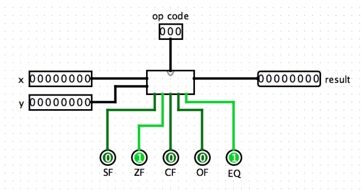
Circuit Layout
Right click on the name of your circuit, main, and choose "Edit Circuit Appearance". If your circuit doesn't look like the image below--a 3 by 6 rectangle with inputs and outputs in the same locations--please edit its appearance so that it does. Again, this will make our grading process much more efficient.
Verify that the inputs and outputs are in the correct places by using your ALU circuit as part of a larger circuit. (You might want to do this when you test the circuit anyway.)
The opcode input is on top, x and y are on the left side with x on top of y, the result is on the top-half of the right side, and the flags are along the bottom. Going left to right the order of the flags should be SF, ZF, CF, OF, and EQ. Remember that if you hover the mouse over a connection point the corresponding pin's label will appear.
There is a QUESTIONNAIRE file for you to fill out and submit with your lab solution. Your answers to the questionnaire will not affect your grade.
Only one member of your partnership needs to git push your solution.
For both part 1 and part 2 you will be pushing files to the same Lab3 repo. Make sure for part 1 you have committed and pushed part1.circ and for part 2 you have committed and pushed alu.circ. The QUESTIONNAIRE is due with part 2.
Troubleshooting
If git push fails, there are likely local changes you haven't committed. Commit those first, then try pushing again:git add part1.circ git add alu.circ git add QUESTIONNAIRE git commit git push
The push will also fail if your partner pushed, but you have not pulled their changes. Do a git pull. Run `make` and test that your circuits still work. Then you can add, commit, and push. If this doesn't work, take a look at the "Troubleshooting" section of the Using git. You may need to do a merge. After the merge, test that your circuits still work before submitting.